Moria Kwiat, Shimrit Cohen, Alexander Pevzner, Fernando Patolsky

Nano Today, (2014) 8, 677-694
Abstract
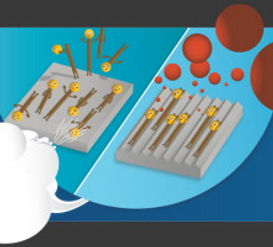
One of the most difficult problems facing the integrated circuit industry is that conventional top-down strategies, which have been the methods of choice for decades, have almost reached their limit. With the industry quest for smaller electronic devices of higher functional complexity based on nano-technologies, which are faster, more portable and less energy-consuming, intensive efforts for solutions based on bottom-up strategies are currently invested. A major difficulty that challenges the creation of functional high-performance devices based on bottom-up grown nanostructures is the accurate deterministic positioning of the individual nanostructures into large perfectly aligned arrays, in a similar manner to top-down strategies. Two main approaches are chosen to solve these issues, involving post-growth assembly-based methods or grow-in-place assembly-free methods. This review provides an overview of the most recent developments in this field, with present perspective concerning their applicability as industrial processes, concentrating on the assembly of one-dimensional nanowires and nanotubes structures. Another route is devised that combines top-down and bottom-up strategies for the on-place NWs growth in a single step, exploiting the strengths of both approaches. Although major advance is shown in the field, it is concluded that current methods are still lacking on their way to become high throughput, industrial-scale manufacturable, and potentially can be covered by a hybrid approach, integrating top-down techniques with grow-in-place assembly-free growth methods.

